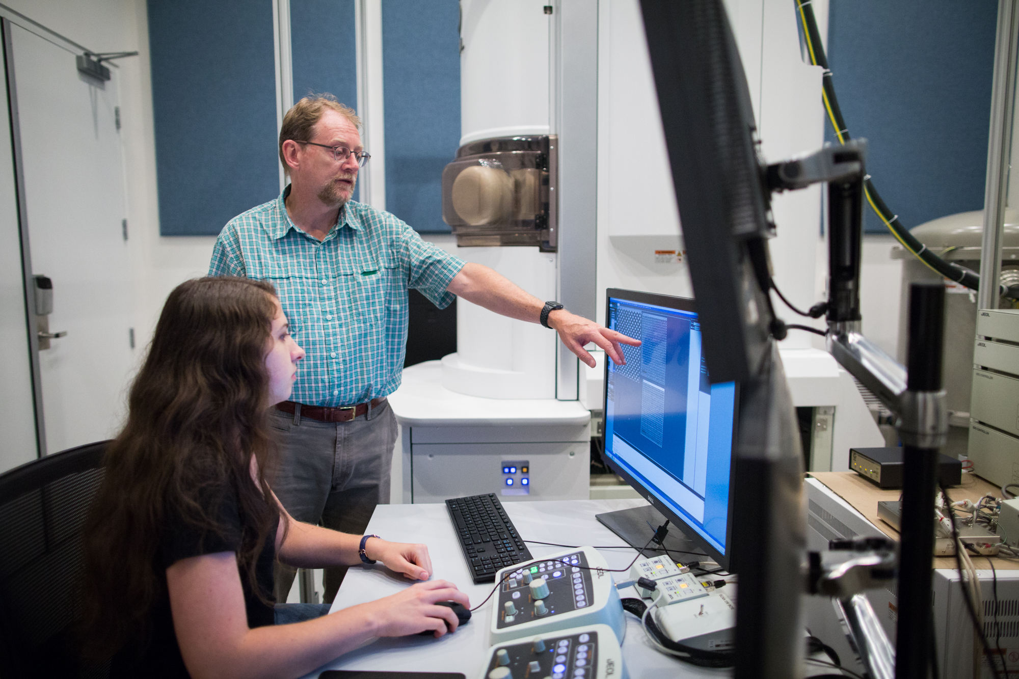
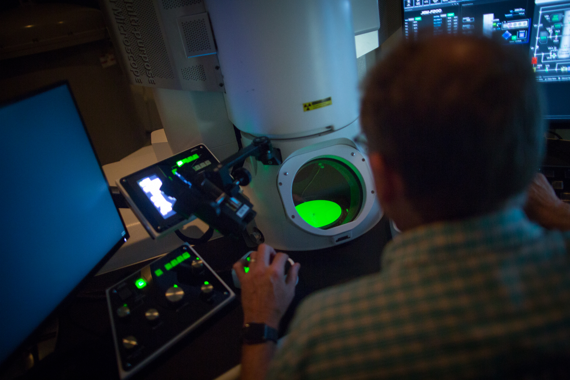
Standing beneath a pearly white, towering microscope called the JEOL NEOARM, Penn's Douglas Yates explains that scanning transmission electron microscopes are so powerful they can image down to the atomic level. These microscopes fire energetic electrons through the object being examined. This allows researchers to create an atomic-scale image through the interaction between the electrons and the atoms in the sample.
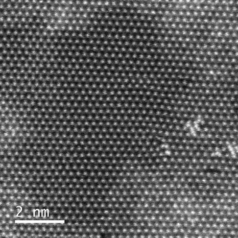
Penn’s NEOARM is the first in the United States. “This instrument is unique because it reaches the sub-angstrom level, down to 78 picometers,” says Yates, director of the Nanoscale Characterization Facility in Penn’s Singh Center for Nanotechnology. “We’re now in the sub-nanometer realm.”
Scientists at the Singh Center can now use two of these advanced microscopes: the NEOARM, and another called the F200. The F200 will be used for most material analyses, while the NEOARM will be used for viewing objects at the highest possible magnification at a low electron voltage. The microscopes will support research, including projects funded by the National Science Foundation’s Materials Research Science and Engineering Centers program, which is headquartered at Penn’s Laboratory for Research on the Structure of Matter.
“These microscopes will enable Penn researchers and external users alike to develop critical understanding of materials and structures in broad fields, including quantum materials, soft matter, catalysts, optics, electronics, metals, and ceramics,” says Mark Allen, scientific director of the Singh Center and the Alfred Filter Moore Professor of Electrical and Systems Engineering in the School of Engineering and Applied Science. “This investment significantly enhances the research enterprise across the University, nearby institutions, and companies.”
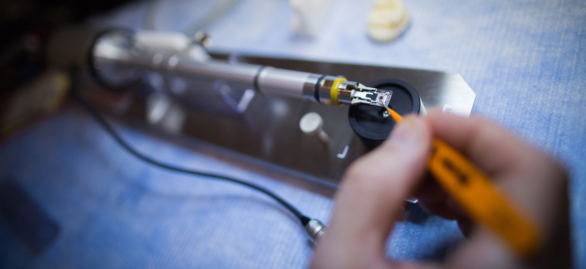
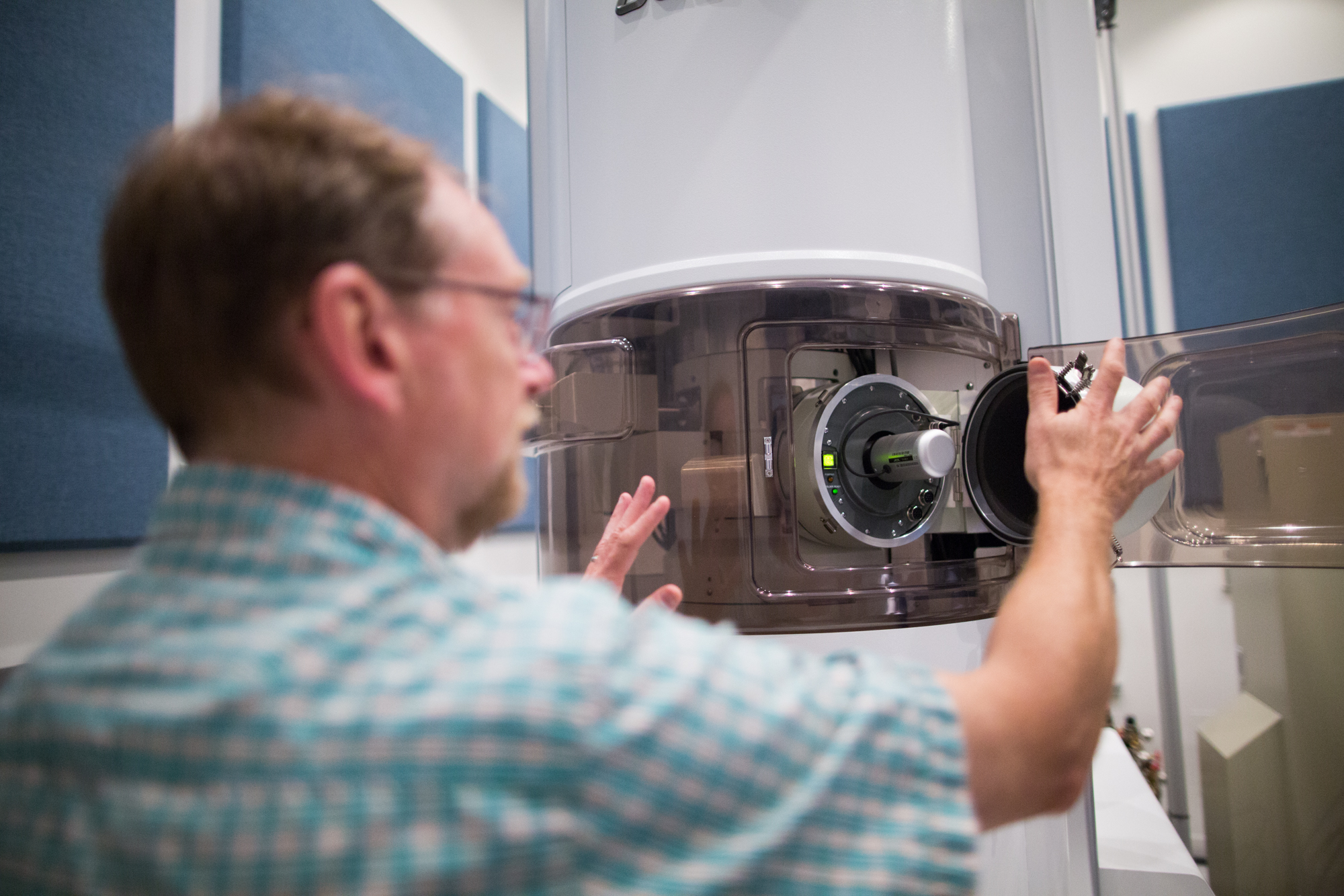
Yates demonstrates how to load a material sample, opening the sample holder and then sealing it. He describes how to prepare the system to analyze the sample to Nicole Bohn, a senior from Enola, Pa., and a science, technology and society major. Bohn, who’s also pursuing a minor in materials science and engineering, trains researchers on how to use traditional scanning electron microscopes.
“The electron gun generates a beam of electrons, which is projected onto a thin sample. The interaction of the electrons with the atomic structure of the sample generates an image, which is magnified and projected onto a fluorescent screen or camera,” Yates explains.
The resulting image allows researchers to see spaces in between atoms. A critical understanding of such small details has big implications in fields such as material characterization and nanotechnology, particularly in the race to develop advanced soft matter materials, such as graphene, a one-atom thick sheet of carbon atoms arranged in a hexagonal lattice, like chicken wire. Though it’s extremely thin, layered graphene is so strong that it can be used in body armor, but so energy-conducive, lightweight, and flexible that it can be used in solar cells, medical devices, and more. These microscopes, the NEOARM in particular, will allow Penn researchers to test and study graphene and other materials with unprecedented precision.
“We are excited to bring these world-class capabilities in materials characterization to Penn and the Singh Center,” says Kathleen Stebe, Penn Engineering’s deputy dean for research, and the Richer & Elizabeth Goodwin Professor of Chemical and Biomolecular Engineering. “These microscopes provide record resolution at low-electron voltages, and therefore minimal sample damage.”
Minimal damage is key when analyzing 2-D materials like graphene. Low-voltage electrons allow researchers to control their sampling, while high-voltage electrons would knock atoms out of place. Some nanotech research projects at Penn require pinpoint precision for creating purposeful notches or holes in a material to understand how “defects” can be beneficial, so low-electron imaging is crucial.
Lower voltage electrons also allow researchers to better study soft matter, such as liquid crystals, polymers, and some biological structures. Soft matter materials are mostly comprised of elements like carbon and hydrogen, and because low voltage electron imaging can produce quality contrast images, researchers can create an especially clear image of a sample.
“In the past, the way we’ve been able to increase the resolution of [transmission electron microscopes] is to increase the voltage of the electrons,” says Erich Stach, a professor in the Department of Materials Science and Engineering. “The problem there is that the more energetic the electrons are, the more likely you are to damage the subject.”
Traditional electron microscopes require upward of 300 kiloelectronvolts (KeV) to produce high-resolution images. Thanks to the scanning electron microscopes, that’s no longer a problem. The NEOARM requires just 30 KeV for high-quality resolution.
“There is still much to be understood about how to best exploit this new capability for soft matter,” Stach says. “This will be a subject we’ll be exploring as students get going with the instrument.”
JEOL, the manufacturer of the F200 and NEOARM, teamed up with Penn partly because it brings their newest technology to a wide audience.
JEOL representatives attended a symposium at the Singh Center on Aug. 10 to dedicate the microscopes, an event that featured presentations from Singh Center researchers, JEOL representatives, and nanoscientists from all over the country.
“Penn has been home to JEOL microscopes for more than 40 years,” says Tom Isabell, director of product management at JEOL USA. “We’re excited to expand upon this relationship and push the boundaries of nanotechnology. It is an honor to have these world-class instruments in the hands of world-class researchers at a peerless university like Penn. These transmission electron microscopes will be taken to their limits and will show what they are fully capable of.”
Homepage photo: Two high-resolution microscopes housed at Penn’s Singh Center for Nanotechnology will allow researchers to study materials at the atomic level. The scanning transmission electron microscopes will enhance research involving quantum materials, soft matter, and more.