Topological insulators are a game-changing class of materials; charged particles can flow freely on their edges and route themselves around defects, but can’t pass through their interiors. This perfect surface conduction holds promise for fast and efficient electronic circuits, though engineers must contend with the fact that the interiors of such materials are effectively wasted space.
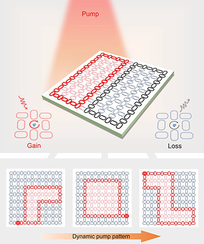
Now, Penn researchers, who first discovered topological insulators in 2005, have shown a way to fulfill that promise in a field where physical space is at an even bigger premium: photonics. They have shown, for the first time, a way for a topological insulator to make use of its entire footprint.
By using photons instead of electrons, photonic chips promise even faster data transfer speeds and information-dense applications, but the components necessary for building them remain considerably larger than their electronic counterparts, due to the lack of efficient data-routing architecture.
A photonic topological insulator with edges that can be redefined on the fly, however, would help solve the footprint problem. Being able to route these “roads” around one another as needed means the entire interior bulk could be used to efficiently build data links.
Researchers at Penn’s School of Engineering and Applied Science have built and tested such a device for the first time, publishing their findings in the journal Science.
Read more at Penn Engineering.