We live in a world of waves. The radio waves hitting your car’s antenna and the light coming in through its windshield, the X-rays that can detect a tumor, and the gamma radiation that can destroy it are all different facets of the same phenomenon: electromagnetism. As one of the fundamental forces of nature, its imprint can be felt on almost everything in the universe.
The difference between these waves that permeate the everyday aspects of our lives is where they fall on the electromagnetic spectrum, meaning how long it takes for each of these waves to crest, fall, and repeat. The waves carrying a radio broadcast might, for example, be a few meters long, large enough to swerve around obstacles on their way to your receiver. The light waves reflecting off these printed words and into your eyes are a few million times smaller than that, and radioactive gamma waves are a million times smaller still.
Mastering the movement of these waves is at the heart of much of modern technology, and at Penn, no one has accomplished that quite like Nader Engheta.
The H. Nedwill Ramsey Professor of Electrical and Systems Engineering at the School of Engineering and Applied Science, Engheta is a leading figure in the nascent field known as metamaterials. Combining several branches of physics and engineering with a healthy dose of nanotechnology, the discipline is focused on creating human-made features that can bend and manipulate waves in ways that nothing in nature can.
Just as a wave’s shape determines its properties, the shape of objects that a wave interacts with can further influence those properties. By designing shapes with features that are smaller than a given wavelength, metamaterials research could potentially develop “super lenses,” which have unprecedented magnification abilities, and “cloaking devices,” which can bend waves around an object, rendering it effectively invisible.
Although it’s been just a little more than a decade since the word “metamaterials” was coined, Engheta is now taking the research to the next level by establishing an even newer discipline he calls “metatronics.” Engheta and his research team recently built the first physical metatronic circuit, which manipulates light waves much the same way an electrical circuit in a computer or phone manipulates electrons.
As if cloaking devices weren’t futuristic enough, metatronics could also lead to the creation of objects that do math when you shine light on them. “What if we could make a material where we put a function in on one end, and get its derivative or integral out on the other? We’re working on that,” says Engheta.
Engheta’s groundbreaking work has earned him a steady stream of accolades, including being named one of Scientific American’s Top 50 Leaders in Science in 2006, and the winner of this year’s IEEE Electromagnetics Award.
Even after three decades of being on the cutting edge of electromagnetics research, Engheta is still motivated by the thrill of the chase, knowing there is always another secret of the universe to unlock.
Q. How did you get interested in electrical engineering? A. I was born and raised in Tehran, and did my elementary school, high school, and undergraduate degree there. I got interested in the field as a kid; I was fascinated by a battery-operated transistor radio. How can we hear music if it’s not connected to anything? I wanted to know how the signal gets from one location, say the radio station, to the radio without being connected to anything. With that curiosity, and knowing that electrical engineering is how I would find out about things like radio waves, I went to the University of Tehran. I came to the U.S. for my higher education, getting a master’s degree and Ph.D. at Caltech. My master’s degree was in electrical engineering and my Ph.D. was electrical engineering with a minor in physics. So I’ve been straddling these two worlds of engineering and physics for a while now. And because I was interested in waves—then microwave waves, and later on optical waves —I got into the field of electromagnetics as a graduate student. My Ph.D. dissertation was on interfacial antennas, which was a big topic in electromagnetics at the time. That led me to my interest in everything having to do with optics, electromagnetics, waves and fields. After my Ph.D., I did a post-doc with my advisor, Charles Papas. He passed away five years ago, but he was a fantastic professor, a great scientist, and a fantastic human being. I learned a great deal from him, not only science, but about humanity. I learned a lot and am indebted to him. After my Ph.D. and post-doc, I worked in industry for four years. I was working on technology related to electromagnetic pulses, which can knock out electrical systems. We were figuring out how they interact with those systems and how we could prevent them from getting in in the first place.
Q. So, when did you come to Penn? A. I came to Penn in 1987, so I’m coming up on my 25th anniversary. Time flies when you’re having fun! I love my job and the research that we do. My wife and I came across the country and established our family here in Philadelphia. My kids were born here.
Q. What were you working on at the time? A. Expanding on my interest in waves, I started building my working group around the idea of electromagnetic wave interaction with chiral structures.
Q. Chiral? A. Chiral structures have handedness, like how your right and your left hand are different from one another. Helical structures—DNA, for example—have chiral properties. My group and I were interested in how we could learn from these kinds of helical structures in nature, and translate it to the microwave frequency. We wanted to see how man-made chiral structures, things like springs, interacted with microwave signals.
Q. So the direction that a spring is coiled makes a difference? A. Exactly. An electromagnetic wave interacts differently with coils of different handedness, because waves have their own handedness. That’s what we call polarization. So if the wave and the coil are both right-handed, the interaction might be one thing, but if one is right-handed and the other is left-handed it could be another thing. This is an example of geometry playing a big role in electromagnetics. In those days, there was a lot of interest into whether we could incorporate these chiral structures into microwave devices, like antennas. We wanted to see if matching those geometries would give us better performance, among other things. Trying to answer those kinds of questions was the precursor to my interest in metamaterials, but it also expanded my interest into a completely different field: biologically inspired optical imaging. There are a number of animal species that can see polarization; many classes of marine species and invertebrates can do this. A dear colleague—Ed Pugh, who was in Penn’s Department of Psychology—was the first person to introduce me to the idea of polarization vision.
Q. But what was the connection, if these two fields were so far apart? A. It all comes down to polarization, which is just one aspect of an electromagnetic field that can interact with structures, natural or man-made, and cause the wave to behave differently. So being interested in waves and fields, polarization vision was something that also interested me. The fact that nature has evolved and can make use of polarization made us ask two big questions: How do these species perceive polarization, and why? In trying to answer these questions, I’ve had a lot of interaction with Penn’s medical school, the Institute of Neurological Sciences, and it’s the reason for my secondary appointment in the bioengineering department here at the engineering school. Ultimately, my interests are about how waves interact with structures, so that got me into the field of complex media, which would be eventually be called metamaterials.
Q. Tell me a little more about how the field of metamaterials coalesced. A. Starting in the late ‘80s, there were several research communities that were working, one way or another, on the issue of wave interaction with structures. Chirality was one of them, but there are also groups in physics interested in photonic crystals—structures with regular patterns—and groups in math interested in symmetry and how it can affect electromagnetics. Towards the year 2000, these groups merged together, which is when the word ‘metamaterial’ really started to be used. Prior to that, each of these subfields was using different terminology and had different motivations. The drive for us was to go into shorter and shorter wavelengths, but everyone was interested in seeing what we could do with this new way of thinking about waves and structures.
Q. What was so new about it? A. It has to do with how man-made materials may have different properties from natural ones. By definition, metamaterials are engineered composite structures that contain collections of small, man-made features, which we call ‘inclusions.’ Engineers can therefore design these inclusions so that the overall structure, the bulk material, gives you wave properties that you’d like to have but aren’t ordinarily found in nature. Nature has given us a lot of natural materials—the whole periodic table and all of the combinations of its elements—and they’re all made out of atoms and molecules. These natural materials have chemical, electromagnetic, and optical properties, all of which are formed by the arrangement of those atoms and molecules. In contrast, the properties of metamaterials are formed by their man-made structural features: their inclusions. These inclusions are much larger than atoms, but they are smaller than the wavelengths we want them to interact with. And because they’re man-made, we can control the properties of those interactions. A hydrogen atom is a hydrogen atom; nature has given us that and we can’t change it. But if we build these inclusions out of different materials and in different shapes, we can have a lot of flexibility. We can fine-tune the properties of the bulk material just like turning a knob. For example, we can control the density of these inclusions, how many we have in a given volume. We can decide what the host medium—the material the inclusions are embedded in—is made out of. We can also control the inclusions’ orientation; whether they are all pointing in the same direction or in random directions. The same goes for distribution, whether they are in a regular pattern or are randomly distributed in the host medium.
Q. Could you give an example of what these inclusions might look like? A. They could be a bunch of metallic spheres embedded in a host medium made out of glass. A sphere is a very basic example; the shapes could be much more complex. The general idea is that being able to control geometry means being able to control waves. The shape of the inclusion and the material it is made out of leaves a footprint on the wave the metamaterial interacts with. As the wave moves through this ensemble structure, it interacts with each of the inclusions individually, producing an effect we call the ‘dipole moment.’ These individual dipole moments all add up, and what you’re left with is the property of the overall structure. In some sense, natural materials work the same way, but those dipole moments occur at the atomic level. Working at a larger scale just gives us control over the effects, leading to the unusual properties metamaterials enable.
Q. What are some of those properties? A. Materials, say, glass or water, have a certain index of refraction. The index of refraction tells us how light, or any wave, will propagate through that material. The higher the index of refraction, the lower the velocity of the wave. With metamaterials, one thing we can do is get an index of refraction that’s negative, which essentially makes the wave go through the material backwards.
Q. What does a backwards light wave look like? A. The example one usually gives is what happens when you put a pencil in a glass of water. When you look at it from the outside, the pencil looks broken. When the light goes through the water, it’s refracted, which makes it reach your eye at a different angle. But if the pencil were inside a metamaterial with a negative index of refraction, it would look like it’s broken in the opposite direction. That by itself has a lot of interesting byproducts and implications. For example, if one had such a material, one would be able to layer the structure in such a way to focus light with a flat lens. Rather than having the refraction of the lens being due to its curvature, you could have it due to the inclusions. Metamaterials are ultimately a way of thinking about how we can tame and control waves. We can do that with natural materials by choosing them based on their index of refraction or by changing their overall shape, but with metamaterials, we can bring other dimensions in play. By having the inclusions arranged in a certain way, you can get a wave to bend and move in the direction you want. When you have building blocks that can be put together in different ways to control the orientation and intensity of the wave, that can open up a lot of interesting possibilities.
Q. The one possibility that gets mentioned a lot with metamaterials is a cloaking device. Would something like that actually work? A. Cloaking is one of the many applications for metamaterials. It gets a lot of attention because of its connection to science fiction, but it’s just one example of many exciting things you can do. To understand how a cloaking device would work, we need to understand how we see objects. We see something when a wave, in this case light, hits an object. The object scatters the wave, some of which comes back and hits our eyes. This goes beyond the visual definition of ‘seeing.’ With the right detector, any kind of wave will work the same way. So the question is whether we can design a metamaterial that goes around an object, with properties such that when the wave hits this ensemble, one of two things happen. One is that the wave goes around the object so it doesn’t produce a shadow, and the other is that it interacts with the object and the cloak such that you don’t have scattering from them at all. Our group has been interested in cloaking since 2005, when we started figuring out the conditions it would work in, as well as its limitations: how big a cloaked object could be and what wavelengths it could cloak. So when we say we can make something invisible, it’s only for a narrow range of wavelengths. Even with these limitations, some of the applications are quite exciting. For example, imagine you want to measure a field around an object using a probe, something like an antenna. The problem is that presence of the probe can change the field. But what if we design something to go around the probe, such that it reduces its scattering? The probe would be invisible from the perspective of the field, but it would still be able to measure it.
Q. Almost any kind of sensor or detector is going to involve waves or fields, so I imagine there are lots of possibilities there. A. Right. Being able to tame and control waves would allow us to do something called sub-wavelength microscopy. An ordinary microscope is diffraction-limited; if the distance between two points is smaller than half the wavelength it operates on, those points can’t be distinguished in the image. But if we could put a layer of properly designed metamaterial near the object, we could image finer details. Since we’re interested in working with smaller and smaller wavelengths, a lot of our research could lead to advances in miniaturization, including the miniaturization of circuitry by using light instead of electrons.
Q. That’s the new field you’ve dubbed ‘metatronics,’ right? What is that? A. The ‘meta’ in ‘metatronics’ comes from metamaterials, and the ‘tronics’ comes from electronics and photonics. If you look at the electronics around us, they consist of circuits, which are made out of what we call ‘lumped circuit elements.’ These are things like resistors, capacitors, transistors, diodes and so on. One of the things I’ve been most interested to do with metamaterials is seeing if we can use it to have these circuit elements operate at optical frequencies.There are a lot of advantages to that. You can make circuitry with very small volumes, helping with miniaturization. You can also get higher data rates; working with photons is faster than with electrons.
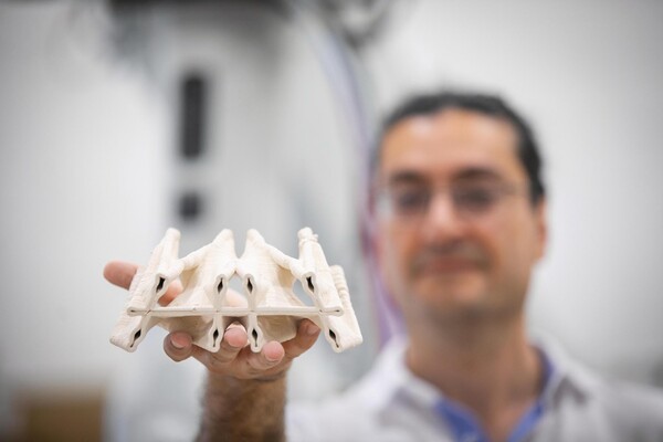
Q. But the circuitry in, say, a computer chip is already incredibly tiny and fast. Will this really make a difference? A. It’s the difference of several orders of magnitude. With smaller distances the signal has to travel over, your input gets converted to output much faster. It would be a new paradigm in information processing with new filtering, signaling, and switching properties, maybe amplification and data storage. We first introduced the idea in 2005: under the right conditions, nanoparticles can act as an optical capacitor, optical resistor, and optical inductor, counterparts to what we have in electronics. We extensively studied the theory, figuring out how we would connect these circuit elements together. After many computer simulations, we conducted an experimental realization and verification of the theory. We’ve just published a paper in the March issue of Nature Materials that describes that experiment.
Q. What did you physically make for that experiment? A. Using nanofabrication, our group built structures made of suspended arrays of silicon nitrite nanorods with precisely spaced gaps between them. When an infrared light wave passes through these comb-shaped structures, the rods and gaps interact with the wave, and the system acts like circuits with an inductor, capacitor, and resistor at infrared wavelength. Each of those nanorods are less than 250 nanometers wide, and the gaps are even smaller; they have to be much smaller than the wavelength of the infrared light we used.
Q. So nanotechnology plays a big role in this research? A. Nanotechnology is currently able to produce the materials we need for this wavelength, but as we move into the future with smaller and smaller wavelengths, the requirements become more stringent. We’ll need greater precision in positioning increasingly small nanostructures next to one another, but it’s something I’m very hopeful that will continue to evolve. That’s an interesting challenge for metatronics; how to connect particle ‘A’ to particle ‘B’ with a precise direction. It’s not as if we can just solder them together with wires, like in electronics. Just like with any technology, the first generation will have some variation in results, because of imperfection in manufacturing. But as the technology evolves, you can make it more and more precise, which we’ll need for some of the most interesting features of metatronics. One of the most beautiful aspects of metatronics is that depending on the orientation of the light polarization [with which] you excite the circuit, the behavior of the circuit can change. It’s as if we could rewire an electronic circuit while it’s embedded in a device. That phenomenon gives you a multiplicity of functionalities in the same physical structure. In fact, the same metatronic circuit could act as two different circuits at the same time.
Q. So that would also open possibilities of new kinds of smaller circuit designs, because you could fit twice the number of circuits in the same amount of space? A. Yes, but that’s not all. Metamaterials helped us come up with the idea of metatronics, but this directional aspect of metatronics might allow us to build much more exotic kinds of metamaterials. Imagine if we put many metatronic circuit structures next to one another, just like we arrange inclusions in the host medium of a metamaterial.
Q. We’d get a meta-metamaterial? A. Exactly! Your bulk material is going to look completely different from different directions.
Q. What are the next steps before metatronics leaves the lab? A. I see the evolution of metatronics as being very similar to that of electronics. We’re working on expanding the field, so we’re looking into the possibility of making switches, three-port elements, such as transistors, and making metatronics digital, instead of analog. In electronics, when we have a signal that varies over time, it’s analog, but when we just have 1’s and 0’s, it’s digital. I’m very interested in translating this concept to light; developing particles and elements that will react to light being present or not, rather than varying by the amount of light. That would very much help the signal-to-noise problem, and help to expand the concept of metatronics into the world of logic elements. If we get to that point, it would allow us to do calculations and information processing. Nanoscience is going to play a big role in that, especially the localization and orientation of these elements.
The Polyhedral Structures Laboratory is housed at the Pennovation Center and brings together designers, engineers, and computer scientists to reimagine the built world. Using graphic statics, a method where forces are mapped as lines, they design forms that balance compression and tension. These result in structures that use far fewer materials while remaining strong and efficient.
From ancient tombs and tiny robots to personalized gene editing and AI weather models, Penn’s 2025 research portfolio showed how curiosity—paired with collaboration—moves knowledge into impact and stretches across disciplines and continents.
Centering joy in AI development and implementation
PIK Professor Desmond Upton Patton—of Annenberg and SP2—and collaborators introduce a joy-informed framework designed to initiate conversations among engineers, designers, and researchers.
Reflecting on Jane Austen, 250 years after her birth
English professors Michael Gamer and Barri Joyce Gold have been teaching courses specifically dedicated to Jane Austen for years. They spoke with Penn Today about their approach to teaching her novels, how they challenge common readings and myths, and what makes Austen’s work so enduring—and adaptable to the screen—more than two centuries later.
Electronic medical records help save lives of HIV patients
Wharton’s Leandro “Leo” Pongeluppe and colleagues found that HIV clinics in Malawi that switched from paper to electronic medical records saw an estimated 28% reduction in deaths in five years.