(From left) Doctoral student Hannah Yamagata, research assistant professor Kushol Gupta, and postdoctoral fellow Marshall Padilla holding 3D-printed models of nanoparticles.
(Image: Bella Ciervo)
A gleaming new Penn facility is poised to help researchers continue to make an impact in the field of nanotechnology. The Krishna P. Singh Center for Nanotechnology, which officially opened on Oct. 4, is the University’s new home base for research, education, and public-private partnerships focused on the manipulation of matter on an atomic and molecular scale.
The Center, which is a joint venture between the School of Engineering and Applied Science and the School of Arts & Sciences, is Penn’s first collaborative building between two schools. Faculty from both schools will use the building’s state-of-the-art resources to do two things, according to Mark G. Allen, the inaugural scientific director of the Singh Center: Build and measure.
[flickr]72157636192231736[/flickr]
“This will allow researchers to make significant strides in their work,” says Allen. “Now that we have the building and the infrastructure and the physical space for it, we have new functionalities that didn’t exist before.”
The 78,000-square-foot building, designed by the New York City-based Weiss/Manfredi Architecture/Landscape/Urbanism firm, contains two suites, one for nano-characterization and the other for fabrication.
Both tasks demand a pristine environment, free from vibrations from nearby bus or trolley traffic and certain wavelengths of light. To that end, the 10,000-square-foot characterization facility is situated on bedrock 18 feet below the earth’s surface to minimize vibrations that would interfere with atomic and electron microscopes. The labs are also designed to be isolated from temperature fluctuations, atmospheric turbulence, and electromagnetic noise.
The 10,000-square-foot fabrication room, which is located behind the Center’s ground floor signature marigold glass wall, contains a cleanroom. There, researchers can use assembly tools to grow carbon nanotubes, deposit graphene, and etch microelectronic systems.
The Center also contains a large existing suite of equipment for nanotechnology research, including electron and scanning probe microscopy, electron beam lithography, and space for the first aberration-corrected, energy-filtered microscope in the greater Philadelphia area.
Allen says researchers will be able to use the Center’s facilities to look at new electronic materials with enhanced functionality. In addition, the Center will allow researchers to merge the electrical and mechanical, making even-smaller versions of items that could lead to the next handheld device breakthrough.
He adds that Penn has an opportunity to make a huge impact at the intersection of medicine and nano-fabrication technologies.
“That is an area where Penn has an opportunity to be a differentiating factor because of the strengths of both the [Perelman School of Medicine] and the Engineering School,” Allen says. “This could range from things like in vitro diagnostic or point-of-care devices to be able to more quickly and easily analyze blood or other fluids in either a doctor’s office or in a country that doesn’t have widespread medical resources.”
Allen hopes to open up the Center not just to nano researchers, but those in schools across the University.
“I would love to see our electron microscopes used not only to figure out the structure of matter, but also to see what might be learned about things that are in the basement of the [Penn] Museum,” Allen says. “That could be really interesting.”
Allen and his staff will also be reaching out to research communities outside of the University to increase partnerships with other schools, as well as between Penn and private companies. Companies—especially those too small to afford some of the equipment housed at Singh—will be able to send their employees to the Center to engage in exploratory research or build prototypes.
“The other thing that Penn offers is ... not only the infrastructure equipment, but the infrastructure of ideas,” Allen says. “There’s such a breadth of expertise at Penn that if the industry needs a particular problem solved or would like a brainstorming session about what’s next in nanotechnology, then there is a tremendous resource here.”
The full potential of the building will be phasing in through 2014. Allen, a recent transplant from Georgia Tech and a pioneer in the field of micro-electromechanical systems and nanofabrication technology, will be moving his lab into the space early next year.
“We’re open for business, both the business of ideas, as well as the fabrication and characterization equipment,” says Allen. “We want to interact with as broad a cross-section of the University, as well as the Philadelphia area, as we can.”

(From left) Doctoral student Hannah Yamagata, research assistant professor Kushol Gupta, and postdoctoral fellow Marshall Padilla holding 3D-printed models of nanoparticles.
(Image: Bella Ciervo)

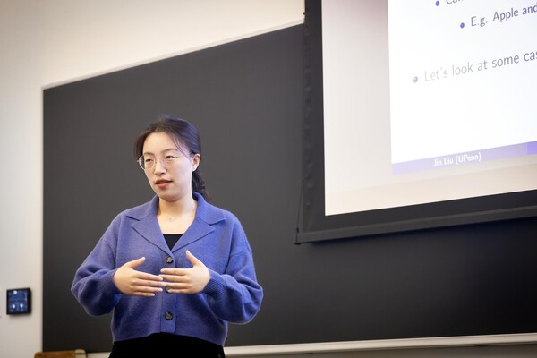
Jin Liu, Penn’s newest economics faculty member, specializes in international trade.
nocred

nocred

nocred