Moore than meets the eye: The evolution of computing
Benjamin C. Lee of the School of Engineering and Applied Science shares five things to know about the evolution of microchips and how Gordon Moore’s scaling laws set the pace for making our devices faster, cheaper, and smaller.
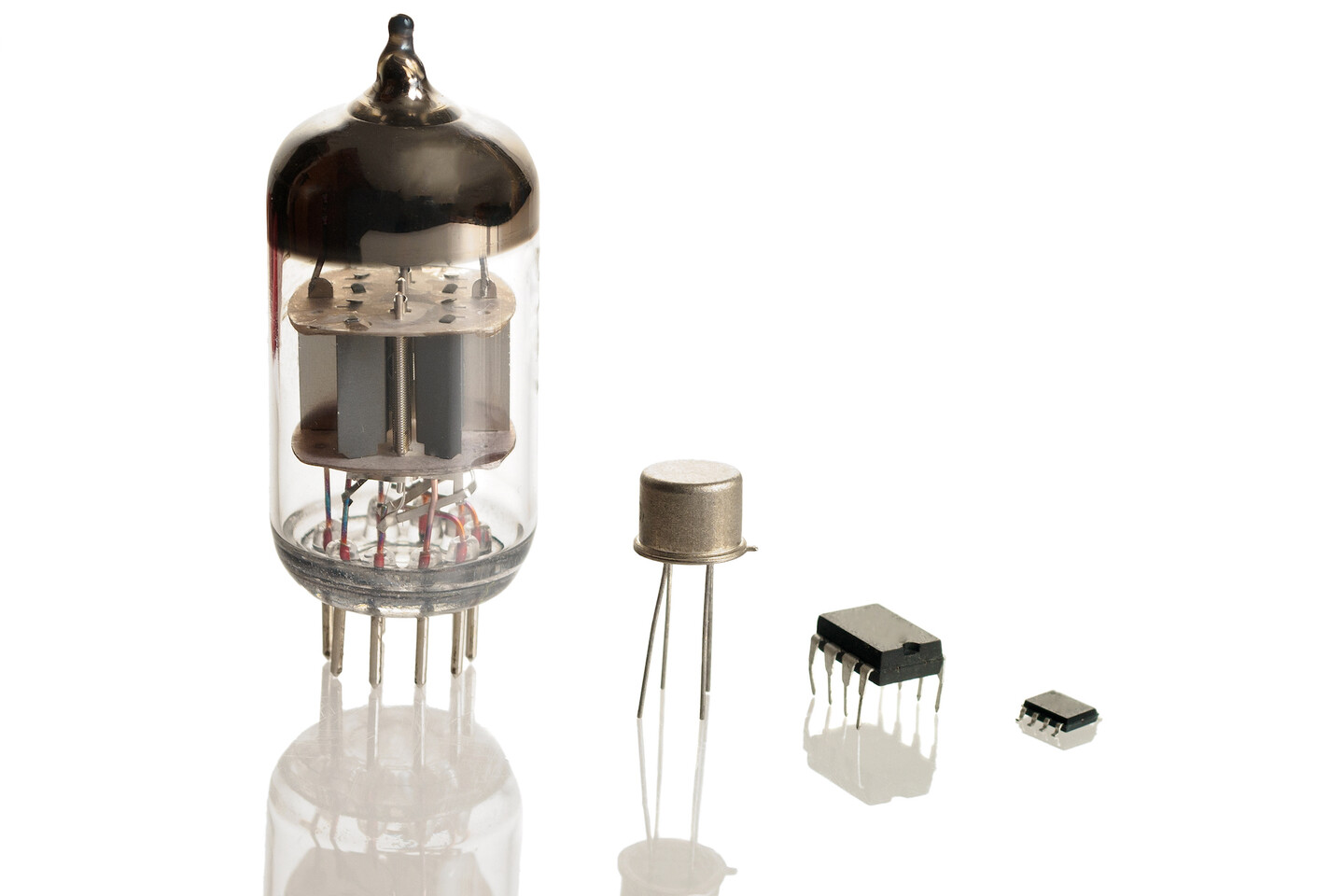
Transistors replaced vacuum tubes in the mid-20th century. They were initially made of germanium and later silicon, leading to the development of integrated circuits containing millions to billions of transistors on a single chip. The Metal-Oxide-Semiconductor Field-Effect Transistor (MOSFET) became the dominant type due to its smaller size, faster speed, and greater energy efficiency. Today, MOSFETs are essential components in modern electronic devices such as computers, smartphones, and power electronics.
(Image: iStockphoto/vlabo)
Following the global supply chain collapse brought on by the COVID-19 pandemic, it became obvious that many facets of modern life are surreptitiously ruled by a tiny piece of technology known as the semiconductor chip. From our phones and fridges to fighter jets, these small, flat pieces of semiconductor material play crucial roles in facilitating data processing and storage.
Though chips are seemingly ubiquitous, they are deceptively complex. At the heart of the evolution of these tiny but increasingly powerful technologies lies a principle known as Moore’s law, named for Gordon Moore, an engineer who co-founded Intel Corporation. Penn Today spoke with the School of Engineering and Applied Science’s Ben Lee to discuss the rapid evolution of computers and to reflect on the seminal work of Moore, who died in March.
A brief history of chips
The story of chips begins, Lee says, in Silicon Valley in the late 1950s, when engineers began exploring a special characteristic of silicon.
“It’s an excellent semiconductor material,” Lee says, “because it has the ability to partially conduct electrical current, which makes it great for working with electrical components such as transistors, the on-off switches that relay information as ones or zeroes and form the basis of computing.”
By the early 1960s, engineers at technology company Fairchild Semiconductor were trying to figure out ways to increase the capabilities of computers by adding more and more transistors to the semiconductor chips that processed and stored their information. One figure who came to prominence in this space was Gordon Moore.
“Moore was a Fairchild co-founder who went on to co-found Intel and famously observed that the number of circuit components you could put on a chip would double at a fixed rate, around every 18 to 24 months,” Lee says. “This came to be known as Moore’s law, which has set the cadence for modern advances in computing from 1965 into the mid-2000s.”
Moore’s original observation was an economic and empirical one, Lee says. Moore argued that component integration reduces costs, and, over time, the most cost-effective integrated circuits are those that integrated more and more components. This observation has held true for several decades and has been a driving force behind the rapid advancement of computer technology.
How they keep getting better
Lee notes that a phenomenon called Dennard scaling played a major role in shaping chip evolution.
“A chip designer from IBM, Robert Dennard, proposed a set of guidelines to make transistors smaller,” Lee says. “Dennard argued that operating voltages should scale down with transistor dimensions, allowing chips to shrink both in size and power consumption.
“So, riding on the coattails of smaller transistors that allowed you to put more of them on a single chip, we got faster, more energy-efficient, and capable computation and memory,” Lee says. “And all of this happens from generation to generation at an unprecedented pace. It would be like having airplanes that got two times quicker every iteration.”
Lee points out that the cadence laws held for much longer than Dennard or Moore anticipated. In the mid-2000s, however, they began to gradually slow down as the structures needed to keep up with processing demand began to challenge the laws of nature.
The physical limits on how small transistors can be stem from several factors, some of which are at the subatomic level, like subthreshold current, wherein electrons “leak” through the thin barriers in the transistors. Such a circumstance can cause problems in power and reliability, Lee says.
“So, as a result, Intel and others started developing a series of ‘ad hoc design techniques’ to get from one generation to the next,” he says.
To improve performance without greatly increasing power consumption, chip designers employed new transistor designs, Lee says, essentially switching from the industry-standard flat, planar structure to a more three-dimensional design, incorporating a vertical geometry to help control the movement of electrons.
“The fabrication technique behind the most sophisticated transistors is often defined by its process node,” Lee says. “It’s a number that refers to the minimum size of the transistors or other components on a chip. The smaller the number is, like five versus three nanometers, the more sophisticated and powerful the chip is. These numbers have become a way to track the progress of chip technology.”
How transistors get to chips
Lee explains that the chip-making process often begins in the United States or United Kingdom, with firms like Apple and Arm, developing chip design. In many instances, these blueprints are then sent to a company in Taiwan, known as Taiwan Semiconductor Manufacturing Company (TSMC), which essentially “prints,” or fabricates, 300-600 of these designs onto round silicon wafers, usually around a few hundred square-millimeters in size. Each of the fingernail-sized chips on these wafers can hold as many as tens of billion transistors.
TSMC is special, Lee says, because they currently have the most advanced semiconductor manufacturing capability in the world. They currently fabricate chips at the 5-nanometer scale and are slated to produce the next node at 3 nanometers later this year.
“These metrics no longer directly refer to the actual length or dimensions of transistors on a chip. Rather, they quantify the industry’s progress in fabricating more advanced transistors at some cadence originally inspired by Moore,” Lee says. “But that shouldn’t detract from the fact that transistor technologies at the nanometer scale are major feats of engineering. For perspective, a virus’ diameter ranges between 20 to 400 nanometers.”
Lee explains that advanced semiconductor manufacturing requires scientists and engineers to devise new ways to manipulate materials at the atomic level to sustain an advancing ability to compute.
The chips are then cut from the wafers and sent to various countries in Southeast Asia and China for assembly, testing, and packaging into devices such as mobile phones and computers.
A bit about the printers
“There are two more key processes that underlie the creation of the chips: making the printers and producing their constituent components,” says Lee. “These steps are possibly the most expensive and necessitate a high degree of precision to pull off.”
Producing chips at process node requires what’s known as extreme ultraviolet photolithography, wherein ultraviolet light is emitted from one part of the machine and reflected by a series of mirrors onto a silicon wafer to pattern the chips’ designs. It’s similar to a high-tech stencil, where light is used to draw complex designs on a surface.
“To my understanding, it’s an incredibly complex process, and there’s only one Dutch company called ASML that can make the printers for the cutting-edge chips,” Lee says. “Without those ASML machines, you’re just not going to be able to manufacture chips at the most advanced process nodes.”
Even making the printers is highly specialized, with only a few companies globally that design and produce the parts required. For instance, the German firm Carl Zeiss and Nikon and Canon in Japan provide lenses and mirrors, while Lam Research and Applied Materials in the U.S. supply the etching systems, among other tooling parts.
“Looking back, it seems there’s been a lot of consolidation across firms within key parts of this industry, which created large, indispensable companies focused on specific parts of the manufacturing process,” Lee says.
How hardware advances affect software
The impending shift from a 5- to a 3-nanometer process technology hearkens back to principles Moore and Dennard outlined, Lee says. “Any advance in process technology will allow you to integrate more components onto a single chip, and classically, tighter integration means more computational capabilities and lower packaging costs.”
The reason, Lee says, has to do with freeing up room to add more processing units, or cores, to the chip. He explains that chips contain a type of high-speed memory for frequently accessed data, called cache, akin to the human brain’s short-term memory. Both temporarily store information to carry out complex tasks, and, once complete, that data is either discarded or sent to long-term storage. So, if there is a larger capacity for cache, more operations can be performed on the chip directly.
“Some of these reductions in scale will generate benefits immediately for our software because the hardware needs to move data around shorter distances,” Lee says. These advances could even improve the efficiency of servers in data centers, he speculates.
He clarifies, however, that he doesn’t necessarily believe the shift from 5 to 3 nanometers will lead to a reduction in data center machines in the short term. Instead, it opens doors for having more data stored and processed on a single enclosure versus several interconnected devices, which will drive down the energy cost for cloud-based artificial intelligence applications, while also improving their performance.
“There are a lot of people talking about tiny machine learning,” Lee says. “The idea here is that you can shrink a model, or the essence of a model, so that it can fit in your handheld device.
“Now, you’re not going to get ChatGPT-like abilities on your phone, but there is a case to be made that you could someday have chips that seek to emulate the behavior of neurons, neuromorphic accelerators, running scaled-down versions of AIs used for pattern recognition or anomaly detection, all on a smaller device.”
Closing remarks
Progress in semiconductor fabrication will continue to influence supply chain management and foundational technologies. Yet computer architects and chip designers will need to translate these technologies into high-performance, energy-efficient systems that support tomorrow’s software applications.
“Researchers have repeatedly predicted the end of Moore’s law and technology scaling, only to be surprised by continued advances in fabrication technology,” Lee says. “Even so, chip designers have begun exploring ‘Beyond Moore’ strategies to deliver continued growth in performance and power efficiency through better design that is customized for specific classes of computation and through qualitatively new technologies that look beyond today’s transistors and circuits.”
When the Schuylkill swallowed the city: Lessons from Hurricane Ida’s historic flood
New Penn research shows that Hurricane Ida wasn’t a once-in-a-century anomaly but a preview of how climate change, urbanization, and aging infrastructure are rewriting flood risk.
The Fed explained: What it does and why it matters
Former Philadelphia Fed President Patrick Harker and financial historian Peter Conti-Brown, both Wharton professors, unpack the central bank’s origins, its unusual structure, and the quiet ways it shapes the economy
How population changes are impacting primary education worldwide
Research from Penn sociologist Emily Hannum and colleagues reveals regional trends in whether school-age populations are increasing, plateauing, or decreasing—and shows how different countries are responding.
A bioengineered bean gum from the lab of Penn Dental’s Henry Daniell is found to reduce the levels of three microbes associated with head and neck squamous cell cancer to almost zero, without affecting the beneficial bacteria normally found in the mouth.
Fighting oral cancer with bioengineered chewing gum
Research led by Penn Dental’s Henry Daniell shows that antiviral and antibacterial chewing gums reduce the levels of three microbes linked to worse outcomes in oral cancers, paving the way for more effective and affordable therapies.


